
Heterogeneous Integration: Unlocking Performance Gains in Next-Gen Semiconductors
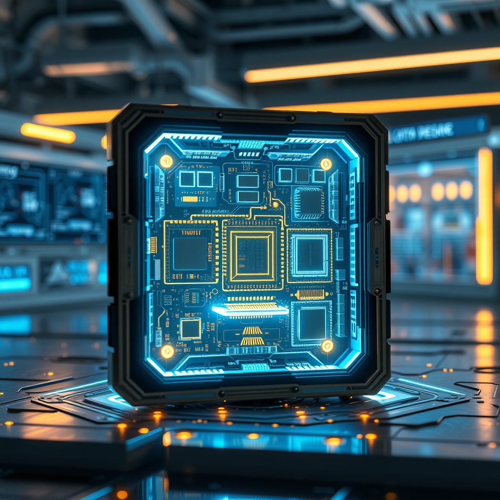
The relentless pursuit of faster, smaller, and more efficient electronic devices has led the semiconductor industry to a pivotal innovation: heterogeneous integration. This approach transcends traditional chip design by combining disparate components—such as logic processors, memory modules, sensors, and even analog circuits—into a single, compact package. The result is a leap in performance, energy efficiency, and functionality that is reshaping industries from artificial intelligence to telecommunications and beyond.
The Driving Forces Behind Heterogeneous Integration
The demand for heterogeneous integration stems from the limitations of conventional monolithic chip designs. As Moore’s Law slows and the physical constraints of silicon become more pronounced, engineers are turning to alternative strategies to sustain performance gains. Heterogeneous integration offers a solution by enabling the coexistence of multiple technologies—such as CMOS, FinFET, and emerging materials like gallium nitride (GaN) or silicon carbide (SiC)—within a unified system. This not only extends the lifespan of existing semiconductor processes but also unlocks new capabilities that were previously unattainable.
One of the most compelling advantages of this approach is its ability to optimize each component for its specific function. For example, a high-performance logic chip can be paired with high-bandwidth memory (HBM) in the same package, reducing latency and power consumption compared to traditional off-chip connections. This is particularly critical for data-intensive applications like AI training, where the speed of memory access can bottleneck overall system performance. Similarly, integrating sensors directly with processing units enables real-time data analysis in edge devices, a key requirement for autonomous systems and IoT applications.
Transforming Key Industries
Artificial Intelligence and Machine Learning
AI and machine learning workloads are among the primary beneficiaries of heterogeneous integration. The ability to tightly couple processors with memory and accelerators—such as GPUs or TPUs—dramatically reduces the data transfer overhead that plagues traditional architectures. Companies like NVIDIA and AMD have already embraced this approach with their multi-chip module (MCM) designs, where multiple dies are interconnected via advanced packaging techniques like silicon interposers or fan-out wafer-level packaging (FOWLP). These innovations have enabled breakthroughs in deep learning, where the sheer volume of data and computational power required demands unprecedented levels of integration and efficiency.
5G and Telecommunications
The rollout of 5G networks has introduced new challenges in signal processing, power efficiency, and thermal management. Heterogeneous integration addresses these by allowing the co-packaging of RF front-end modules, baseband processors, and power amplifiers into a single unit. This not only reduces the footprint of 5G infrastructure but also improves signal integrity and energy consumption. For example, integrating GaN-based power amplifiers with CMOS logic can enhance the performance of 5G base stations, enabling faster data rates and lower latency—critical factors for applications like autonomous vehicles and smart cities.
Advanced Computing and High-Performance Systems
In high-performance computing (HPC), heterogeneous integration is a game-changer. Supercomputers and data centers rely on massive parallel processing, where the efficiency of interconnections between CPUs, GPUs, and memory can make or break performance. By integrating these components into a single package, engineers can minimize the physical distance between them, reducing signal propagation delays and power losses. This is exemplified by AMD’s Instinct MI300 series, which combines CPU and GPU dies with HBM in a single package, delivering unprecedented performance for scientific simulations and large-scale AI models.
Overcoming Design and Manufacturing Challenges
While the benefits of heterogeneous integration are clear, the path to widespread adoption is fraught with challenges. One of the most significant hurdles is thermal management. Packing multiple high-power components into a confined space generates substantial heat, which can degrade performance and reliability. Advanced cooling solutions, such as liquid cooling or embedded microchannels, are being explored to mitigate this issue, but they add complexity and cost to the manufacturing process.
Another challenge lies in the design and verification of these complex systems. Heterogeneous integration requires seamless coordination between disparate components, each with its own electrical, thermal, and mechanical characteristics. Ensuring signal integrity, power delivery, and reliability across these interfaces demands sophisticated modeling and simulation tools, as well as new methodologies for testing and validation. The industry is responding with innovations in electronic design automation (EDA) software, which now incorporates AI-driven optimization to streamline the design process.
Manufacturing also presents a set of obstacles. Traditional semiconductor fabrication relies on standardized processes, but heterogeneous integration often involves mixing and matching components from different foundries or even different technology nodes. This requires advanced packaging techniques, such as 2.5D and 3D integration, which are still evolving. Companies like TSMC and Intel are investing heavily in these technologies, developing processes like chip-on-wafer-on-substrate (CoWoS) and embedded multi-die interconnect bridge (EMIB) to enable seamless integration of disparate dies.
The Role of Standards and Collaboration
The success of heterogeneous integration hinges on industry-wide collaboration and the establishment of standards. Organizations like the Heterogeneous Integration Roadmap (HIR) and the Open Compute Project (OCP) are working to define guidelines for interoperability, thermal management, and testing. These efforts are critical for ensuring that components from different vendors can work together seamlessly, reducing fragmentation and accelerating adoption. Additionally, partnerships between foundries, packaging houses, and design firms are fostering innovation, enabling the development of new materials and processes that push the boundaries of what’s possible.
As the semiconductor industry continues to evolve, heterogeneous integration stands out as a beacon of innovation, offering a path forward in an era where traditional scaling is no longer sufficient. By breaking down the barriers between disparate technologies, it enables devices that are not only more powerful but also more efficient and versatile. The journey is not without its challenges, but the potential rewards—faster AI, ubiquitous 5G, and more capable computing systems—are well worth the effort. The future of semiconductors is not just about shrinking transistors; it’s about reimagining how we build and connect them, and heterogeneous integration is leading the way.